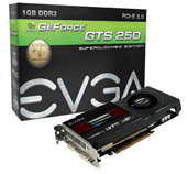
This in-depth Solid Review looks at the EVGA GTS 250. This is a GPU for entry-level gaming that has been surrounded by confusion regarding fabrication process and multiple part numbers that appear to be the same card. Our in-depth look will solidly state the difference between these cards, the truth behind the fabrication process, and extensive overclocking benchmarks.
This GTS 250 article is one of a three part series for entry level, mid level, and high end gaming with EVGA GeForce cards. We will be testing the standard edition 65nm version which is the most ‘entry-level’ GeForce of its series. The mid-level article’s card is a real gem: a 55nm GTX 260 Core 216. The final article is for the new high-end DirectX11 card, a 40nm GTX 470.
I will address fabrication questions on page 2, and then move on to identify all the different versions of the 250. There is a wealth of information in this article, so feel free to use the table of contents to jump around to areas of interest. I have included the full spec list of the 250 series, all available part numbers, FurMark scores, FarCry 2 scores, Crysis scores, temperatures, dimensions, drivers, overclocking potential using the stock cooling and bios settings, overclocking utilities, and other interseting tidbits. We will begin by taking a look at the card used in these tests. This article contains an extensive amount of data. While I have done my best in aggregating it, please let me know if there are any mistakes, so that it may be updated.

GTS 250 in the HAF 922
The Superclocked edition is simply a few Megahertz faster than the standard edition. The “EVGA Precision” tuning tool, which is packaged with your card, can safely and easily do this. If you are still too timid to use it, feel free to pay a few bucks for EVGA to do it for you. For this article’s baseline, we will start at the clock speed of the standard edition and move up from there.
Each benchmark will be ran at both stock and overclocked speeds. Using the EVGA Precision tool, you can dial in any core and memory clock settings you want. By default, the shader clock is linked to the core clock. You can unlink the two and dial in the shader clock yourself. They are linked at the start because the shader clock has to be at least double the core clock. Up next, take a look at the specifications, features, and fabrication size of this card.


