It’s time someone solidly stated the difference between GDDR and DDR. It’s also important to explain GDDR3 vs GDDR5, which are currently the 2 most common forms of memory found in video cards. Both of these topics are popular to discuss, producing plenty of information and misinformation.
In this article, I will explain how GDDR is NOT simply DDR with a G for graphics on the front of it. Then I will discuss the difference between the latest versions of GDDR, which is relevant in today’s GPU market. Along the way, I will attempt to clarify all the confusing terminology that gets thrown around. These terms include “interface”, “bus”, “channel”, “clock cycle”, “width”, “lines”, and “bandwidth.”
Quick Answers for the Impatient
- GDDR is not the same as DDR. Overall, GDDR is built for much higher bandwidth, thanks to a wider memory bus.
- GDDR has lower power and heat dispersal requirements compared to DDR, allowing for higher performance modules, with simpler cooling systems.
- DDR1, DDR2, and DDR3 have a 64 bit bus (or 128 bit in dual channel). GDDR3, comparatively, commonly uses between a 256 bit bus and 512 bit bus, or interface (across 4-8 channels).
- GDDR3 has a 4 bit prefetch and GDDR5 has an 8 bit prefetch, making GDDR5 twice as fast as GDDR3 in apples to apples comparisons.
- GDDR can request and receive data on the same clock cycle, where DDR cannot.
- DDR1 chips sends 8 data bits for every cycle of the clock, GDDR1 sends 16 data bits.

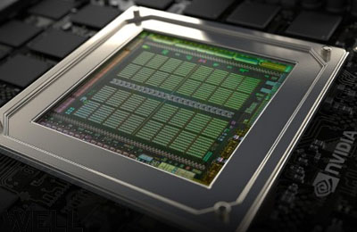
History of GDDR and DDR - courtesy of Samsung
The History- DDR1 and GDDR1
10 Years ago the first double data rate (DDR) RAM was commercially produced in 266 MHz modules. It ran with a 64 bit “memory bus”, just like traditional PC100/PC133 SDRAM, but had double the bandwidth at 2.1 GB/sec. It still operated with a 133 MHz clock, but achieved an effective clock rate of 266MHz by using both the leading and trailing edge of the clock cycle.
This concept of using both sides of the clock cycle actually existed in graphics memory before system memory. It wasn’t until Samsung demonstrated DDR on a mainboard that it was adopted commercially as system memory.
An original DDR RAM chip produced 8 data bits for every cycle of the clock, delivering 8 bits at a time to the I/O data pins. Original GDDR chips delivered 16 data bits for every clock cycle. This meant GDDR could move twice as much data per clock cycle.
Today’s Memory
DDR memory still uses a 64 bit wide bus. Since most of today’s DDR3 system memory is dual or triple channel, this means the overall bus width (or interface) for the system is 128 or 192 bit. Most graphics cards use between 4 and 8 channels, allowing for a memory interfaces up to 512 bit (64 bits per channel x 8 channels).
The large memory buses found in GDDR allow it to transfer large amounts of data on each clock cycle.
Terminology
- Bus – A pathway for data between the memory chips and the memory controller
- Channels – Groups of memory chips. 2 or 3 in system. Usually 4-8 on graphics card
- Clock Speed – Cycles per second, measued in MHz. Every bus has a clock speed and a width
- Data Transfer Rate – Total bits per clock cycle on each pin/wire
- Latency – Clock cycles between data request and receipt
- Data Bus Width – Size of the memory bus, equal to total channels x bits of data per channel
- Interface – Same as data bus width


GREAT site.
Clear, concise, very easy to read, even for an unedumicated person like me.
Thank you very much for your huge amounts of time.
My pleasure Tony. I appreciate those comments!
Hi. I dont know much about hardware but i want to buy a new graphics card and I saw that my current graphics card is ddr.Can I buy a gaphics card that is gddr3?
(more details: i have geforce 6600 and i want to buy geforce 8600 gts 512 mb)
It’s about the slot, not the DDR. Your 6+ year old card came in both an AGP and PCI Express 1.0 version, so your new card would have to match.
However both of those slots (and of course, both cards) are incredibly obsolete. PCI Express 2.0 has been the standard for years now. I suggest you upgrade your system And then get a newer graphics card, even if it’s low end.
You can get a Core i3 2120, matching motherboard, and a bunch of RAM for around $220. Just put those 3 parts in your existing system and you will have a much faster computer.
Actually, yes,i think the slot matches with the new graphics card,i have seen a picture of it. My only worrying was the ddr and thanks for clarifying that, but i will consider the upgrade too. Thank you a lot for your help.
my graphics card is ddr3 and gddr5 what does that mean
It’s one or the other. What card do you have?
Great site, finally someone that states it solidly! I mean seriously, so many people saying “it’s only terminology” others “no, GDDR is x4 times better”. With a friend we were confused, because his GPU is relatively new and has 1gb GDDR5 and we were asking ourselves what’s the difference between DDR5 and GDDR5? Thanks alot 😀
Love to hear it! Thanks
Would it be possible to explain why we can’t use GDDR memory instead of the slower DDR memory as system memory?
Thanks
Jon, there are no technical reasons that I know of not to do this, but there are many logistical reasons.
Higher cost for memory is a factor, followed by having to redesign a spec for mainboards and CPUs (memory controller is on cpu) and other peripherals. Then you would probably have a size consideration since the manufacturing process in nanometers has always trailed behind in GPUs. That would mean messing with the ATX form factor spec. Those reasons together make it unfeasible to create in this market.
Ah I see, ok many thanks for taking the time to reply.
Thank you for simplifying this. I’m shopping for a new video card to do photoshop and was feeling a little lost between the two and the price difference.
You’re welcome!
you answered my question as fast as it took me to ask it. thank you for the straightforward answer and not just saying no one’s better than the other just because you actually gave a reason I can understand and repeat to othersand feel entirely confident I know why. please keep up the good work…
Why can’t we use the faster lower energy and heat GDDR ram chips (from grafics card) that are faster than DDR (ram) in the Ram slots and get a faster speed.
Thank you so much! Even today, no-one explains the differences as succinctly and accurately as you. cheers.
Could you mention the source(s) for your article?
Sorry Amol, this is a really old article and we don’t have that info anymore.
How does SDDR compares with GDDR Rams? Which one is better ?